Working hard on the electronic schematics these days! I’m done with the main B0 current source, finally with less than 3µVPP of noise from 0.1 to 10Hz and 0.4µV of resolution. The voltage-to-current conversion will depend on the shunt resistor, where the worst case is when using a 0R47: the noise and resolution will be of 6µAPP and 0.8µA. I need that much resolution to get the required magnetic field trimming.
I’m also using an NTC close to the current sense resistors, thermally coupled among them and chosen with the same size and PPM/ºC, to compensate by firmware the resistor variations due to self-heating.
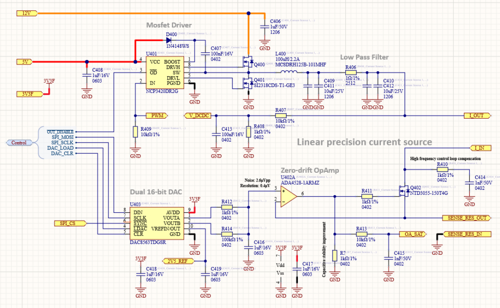
I’m using a DC/DC controlled by the microcontroller to adjust the voltage in the MOSFET drain, and let it work in the linear region. I need the DC/DC because too much voltage across the MOSFET implies too much dissipated power. The main microcontroller will initially perform a calibration:
- 1. Set a current of let’s say 100mA using the 16-bit DAC
- 2. Start increasing the duty cycle of the PWM to rise the I_OUT voltage
- 3. While increasing, keep checking the OA_SAT pin. Right now it will be 3.3V because the small I_OUT voltage makes few current to flow through the coil, and the MOSFET will be in the saturation region. But when the OA_SAT pin becomes <3.3V will mean that we just left the saturation region, so we just need to increase about 0.5V more to give the MOSFET some margin to work properly in the ohmic region without dissipating too much power
A better way would be to connect the I_IN voltage to an ADC input, but it should have to be done through an operational amplifier with low bias current, or the shunt resistor would measure the sum of both currents and the precision would be lost.
A 100µH seems a pretty high value for the DC/DC, but we want the ripple current to be as low as possible. With a so large inductor, we don’t need large capacitors, but what is really important is that they have a low ESR, since that’s the main source of ripple noise. In this case, it’s MUCH better to have a total of 40µF using ceramic capacitors than 470µF using an electrolytic one.
Finally, about the high frequency control loop compensation network. It was added there because we are using a current source to control the current of a VERY large inductor (the one which generates the main B0 magnetic field). Without that network, the operational amplifier would be unstable and it would oscillate.
Let’s keep moving on!